Instructions for Boardview
- Download the latest release of OpenBoardView.
- Torrent or Download the release data, unzip it, and read all included .txt files.
- Open OBV, under View, disable Board Fill and Part Fill, then under File, Open 'Switch Lite Logic Board.bvr'.
- Left-click to view parts/pad nets or click and drag to move, mouse-wheel to zoom, and middle-click or spacebar to flip sides.
What is this?
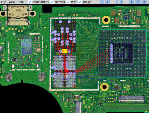
This is the output data for a process I solo-developed for extracting the netlist from an assembled Printed Circuit Board, in this case, a Nintendo Switch Lite logic board. Electrical components are soldered to exposed mounting pads on the PCB, and layers of copper form connections between these pads creating electrical circuits. The full list of these interconnects is called the netlist, and when combined with the part and pad geometries, constitute a boardview. Couple that boardview with reference images of both sides of the PCB, and you have the output data.
How?
There are 3 novel-ish innovations working together to make this happen. They are:
- A process to create geometrical and color-accurate panoramic images of assembled PCBs at 6,000 PPI.
- A point-and-click GUI to draw geometrical part/pad data over the panoramas, with support for adding/modifying other arbitrary data.
- My own PCB capable of powering an arbitrary number of pins one-by-one, reading the state of all pins between each step.
- Take all the images and stitch the bottom-side panorama, flip the board, desolder the RF Shields, then take all the images and stitch the top-side panorama. Use these 2 panoramas and other images against each other to further refine the geometrical and color accuracy.
- Import the completed panoramas into the GUI, and use it to lay down the initial part/pad geometries.
- Desolder every component individually and place them into unique binned locations for future analysis. Record the binned location and presumed reference designator in the GUI, correcting any discrepencies in the pad geometries made in Step 2.
- With all pads exposed and not-shorted, hook one lead of a DMM in continuity mode to the ground plane, and use the other lead to probe every single pad on the PCB. Record all hits into the GUI, merging them into a single net.
- Use the GUI to group remaining pads into net-fragments, based on visual connections in the two outer board layers. If there is no visible connection, assume it is it's own fragment.
- Use the GUI to record the order you solder wires from the extractor PCB pins to which net-fragments on the target PCB.
- Run the extractor. Power goes from the extractor PCB pin, down the wire, into the net-fragment, through all hidden connections in the PCB, into other net-fragments, up those wires, back into the extractor PCB, and are logged to create a complete mapping of all hidden connections.
- Use the GUI to merge all of the fragments into a completed netlist, based on the extractor mapping. Export all this data into a boardview file, pack it up with the panoramas, and then...
- Share and Enjoy.
Limitations
You may have noticed the panoramas are actually at 2,000 PPI. That's because the 6,000 PPI versions are half a gigapixel, each. This causes problems. With everything. You can Torrent or Download them here. Courtesy of ZoomHub, you can now view the top-side and bottom-side panoramas from anywhere!
You may also notice the part/pad outlines are rather simple. That's because the complex rendering feature is currently not supported in OBV. The data is all there, and all files are cross-compatible with the premium, closed-source fork of OBV, FlexBV5.
Step One, post-RF Shield de-solder and Step Seven, pre-extraction, there should be ultrasonic cleaning cycles. It takes many tricks to get the RF Shields off without resorting to using low-melt (bismuth) solder. This is why the top-side panorama is filthy compared to the bottom-side one. There is also some risk pre-extraction that the flux residues can be conductive enough to cause false-positive connections between net-fragments. I don't have an ultrasonic.
There's also a missing step between Step Eight and Nine. That is to take all the parts out of their bins and measure their electrical properties. I have a basic, low-accuracy LCR Meter, but testing them now would result in relatively low-quality and incomplete data.
Why?
My background is over a decade in Electronics Contract Manufacturing serving the medical, aerospace, military, and industrial sectors. More than half of that time is as a SMT Process Technician, with full read/write access to millions of dollars of state-of-the-art equipment. Therein lies the trap: you end up overspecialized, dependant on someone else's unaffordable equipment. Sprinkle in some monthly payments, insurance, ever-moving goalposts, and the mass psychosis of modern corporate dogma; it becomes an elaborate prison.
Using 100% of my willpower to make no further mention of Sisyphus and The Boulder; this project is an experiment in fusing Work-From-Home internet freelancing with master electrical soldering, while still contributing meaningfully to society. I could open a repair shop but that's mostly disassembling and reassembling devices, and troubleshooting electrical circuits. Relatively, very little soldering. Pander to algorithms for ad money? Shill affiliate links? Resell junk tools? Also not soldering. If the goal is to just make money, I could sell 6,000 PPI panoramas of women's feet as NFT's. Note: Do not contact me about this.
So, if you can use this for your own cool stuff, or it saves you time, or makes you money, or if you just think it's neat and would like to see more: please donate. With your help, I can add more devices, reduce cycle time, improve quality, and provide more data while cost-optimizing, documenting, and open-sourcing to make the entire process reproducible.
Contact/Subscribe
Feedback, corrections, and general correspondence is welcome at <second-level domain>@gmail.com. RSS is supported. Alternatively, send an email with 'SUBSCRIBE' as the subject to join the e-mailing list.